
NVIDIA GPU Stack vs Google TPU Stack (2026): Two “AI Factory” Philosophies
The AI infrastructure market in 2026 is no longer “GPU vs GPU.”
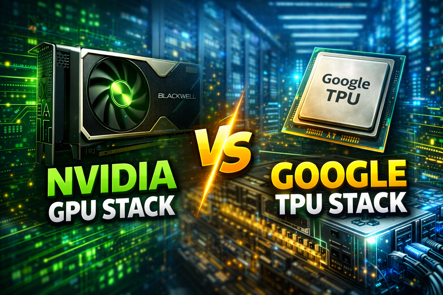
It’s stack vs stack.
NVIDIA sells the most widely adopted general-purpose AI acceleration platform (GPU-first, systemized into rack-scale “AI factories” with NVLink + networking + a massive software ecosystem).
Google sells a vertically integrated TPU platform (custom ASICs, pod-scale interconnect, and compiler/runtime tooling tuned for large-scale training and serving — increasingly accessible on Google Cloud).
If you’re building, buying, or advising teams on AI infrastructure, here’s the clean comparison: what each stack contains, what it’s best at, where the lock-in lives, and how to choose.
1) What each stack actually is
NVIDIA stack (what hyperscalers buy)
NVIDIA’s hyperscale story is “the rack is the computer.”
A modern NVIDIA deployment typically includes:
Compute
GPUs (A100 → H100 → Blackwell / rack-scale systems like GB200 NVL72)
CPU pairing in newer rack designs (Grace-based in those systems)
Scale-up interconnect (inside the rack / NVLink domain)
NVLink + NVLink Switch System (example: NVL72 class designs advertise 130 TB/s GPU communications in one NVLink domain)
Scale-out networking (between racks / clusters)
InfiniBand (Quantum line, including higher-speed generations like Quantum-X800)
Ethernet tuned for AI clusters (Spectrum-X line)
Software
CUDA + libraries, training tooling, and a heavy inference stack (TensorRT / Triton / packaged deployment options like NIM)
The value proposition: maximum ecosystem compatibility + extreme rack-scale density + mature production tooling.
Google TPU stack (what Google Cloud sells)
Google’s TPU story is “pod-scale ASICs + compiler/runtime = efficient scale.”
A modern TPU deployment typically includes:
Compute
Cloud TPUs across generations (v4 → v5p/v5e → Trillium / v6e), tuned for training/fine-tuning/inference
Pod-scale interconnect
TPUs are designed to run in slices/pods with a dedicated inter-chip interconnect (ICI).
Example: TPU v5p documentation lists 459 TFLOPs BF16/chip, 95GB HBM2e, and 1200 GB/s bidirectional ICI per chip (plus large pod sizes).
Trillium (6th gen) is positioned as a big step up vs v5e, with higher compute, doubled HBM capacity/bandwidth, and doubled ICI bandwidth vs v5e.
Software
TPU usage is strongly tied to XLA compilation and supported framework paths.
Google Cloud markets TPUs as supporting PyTorch, JAX, and TensorFlow.
Google has been working to reduce adoption friction for PyTorch users (reported “TorchTPU” efforts).
The value proposition: cost-efficient scaling (especially on Google Cloud) + highly optimized pod architecture + tight integration with Google’s AI platform.
2) Hardware philosophy difference
NVIDIA GPUs: general-purpose acceleration, everywhere
GPUs are flexible and run basically everything (training, inference, graphics-ish compute, HPC).
NVIDIA then systemizes that flexibility into rack-scale architectures (NVLink domains + cluster networking).
Google TPUs: purpose-built ASICs for ML, scaled as pods
TPUs are custom ML accelerators designed around the idea that large models should run efficiently across many chips with dedicated interconnect.
TPU v5p specs show the “pod machine” concept directly in the docs (pod sizes, 3D torus topology, ICI bandwidth).
Trillium/v6e pushes the same idea forward (more memory + more interconnect + better perf per chip vs v5e).
3) Software lock-in: CUDA vs XLA (this is the real battle)
NVIDIA: “default compatibility”
If you’re a typical ML team:
CUDA support is assumed across tools, kernels, and production inference stacks.
Deployment tooling is mature and standardized (TensorRT/Triton, etc.).
Google TPU: “compiler-first performance”
To get TPU performance, you usually embrace:
XLA compilation behavior and TPU-specific execution characteristics (batching, shapes, memory padding considerations, etc.).
The ecosystem is improving, especially for PyTorch users, but it’s still a real adoption variable (Google is explicitly trying to close this gap).
A practical way to say it:
NVIDIA lock-in is “everyone already uses it.”
TPU lock-in is “performance comes from following the TPU path.”
4) Networking and scaling: NVLink domains vs TPU pods
NVIDIA: scale-up + scale-out
Inside the rack: NVLink/NVSwitch creates a huge “scale-up” fabric (NVL72 class = very high intra-domain bandwidth).
Between racks: InfiniBand/Ethernet fabrics move gradients/activations efficiently across very large clusters.
TPU: pod-native scaling
TPU pods are designed around dedicated interconnect topologies (e.g., 3D torus for v5p) and large slice/pod scaling described in official docs.
5) What each is typically best for (real-world patterns)
NVIDIA is usually the best default when you need:
maximum portability across clouds / on-prem
the broadest library + kernel ecosystem
production inference tooling that’s already battle-tested
flexibility to run lots of different workloads without rework
TPUs often shine when you:
are “all-in” on Google Cloud and want cost-efficient scaling
run workloads that fit TPU execution well (common transformer training/serving patterns)
can invest in TPU-optimized code paths (or use frameworks/settings that already align)
want pod-native scale behavior with dedicated interconnect
6) How to choose (a simple decision framework)
Pick NVIDIA if:
your team is PyTorch-first and you need the least friction today
you care about multi-cloud or on-prem portability
your product depends on production inference maturity and debugging comfort
Pick TPU if:
you’re heavily on Google Cloud already (data + pipelines + deployment)
you want optimized training/serving economics and can adapt to TPU constraints
your workload maps cleanly to TPU pods/slices and you can standardize shapes/batching
Many serious teams end up hybrid:
train where it’s cheapest/fastest (often TPU or huge GPU clusters),
deploy inference where portability and tooling wins (often NVIDIA).